Digital Design and Computer Architecture 第二章归纳
0 前言
这一章的布尔方程和布尔代数部分在离散里已经学过了,但是讲的比离散课本好十万甚至九万倍。
Timing部分在数据结构的图里学过。
1 基本概念
Circuit
In digital electronics, a circuit is a network that processes discrete-valued variables. A circuit can be viewed as a black box, shown in Figure 2.1, with
- one or more discrete-valued input terminals
- one or more discrete-valued output terminals
- a functional specification describing the relationship between inputs and outputs
- a timing specification describing the delay between inputs changing and outputs responding.

Circuits are composed of nodes and elements. An element is itself a circuit with inputs, outputs, and a specification. A node is a wire, whose voltage conveys a discrete-valued variable. Nodes are classified as input, output, or internal. Inputs receive values from the external world. Outputs deliver values to the external world. Wires that are not inputs or outputs are called internal nodes.
Nodes A, B, and C are inputs. Y and Z are outputs. n1 is an internal node between E1 and E3.

Combinational and Sequential Circuits
- A combinational circuit’s outputs depend only on the current values of the inputs.
- A sequential circuit’s outputs depend on both current and previous values of the inputs.
To simplify drawings, we often use a single line with a slash through it and a number next to it to indicate a bus, a bundle of multiple signals. If the number of bits is unimportant or obvious from the context, the slash may be shown without a number.
The symbol $C\L$ inside the box indicates that it is implemented using only combinational logic.
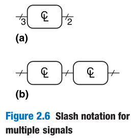
The rules of combinational composition
A circuit is combinational if it consists of interconnected circuit elements such that
- Every circuit element is itself combinational.
- Every node of the circuit is either designated as an input to the circuit or connects to exactly one output terminal of a circuit element.
- The circuit contains no cyclic paths: every path through the circuit visits each circuit node at most once.
2 布尔方程与布尔代数
Terminology
The complement of a variable $A$ is its inverse $\overline{A}$. We call A the true form of the variable and A the complementary form.
The variable or its complement is called a literal.
The AND of one or more literals is called a product or an implicant.
An implicant is called a prime implicant if it cannot be combined with any other implicants in the equation to form a new implicant with fewer literals.
A minterm is a product involving all of the inputs to the function.
The OR of one or more literals is called a sum.
A maxterm is a sum involving all of the inputs to the function.
Order of operations: NOT > AND > OR.
Sum-of-products Form
Sum-of-products canonical form is a Boolean equation for any truth table by summing each of the minterms for which the output is TRUE.
Product-of-Sums Form
Product-of-sums canonical form is a Boolean equation for any truth table by multiplying each of the maxterms for which the output is FALSE.
Attention: Sum-of-products and product-of-sums form do not necessarily generate the simplest equation.
Axioms
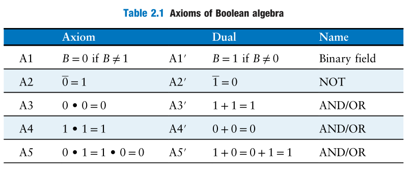
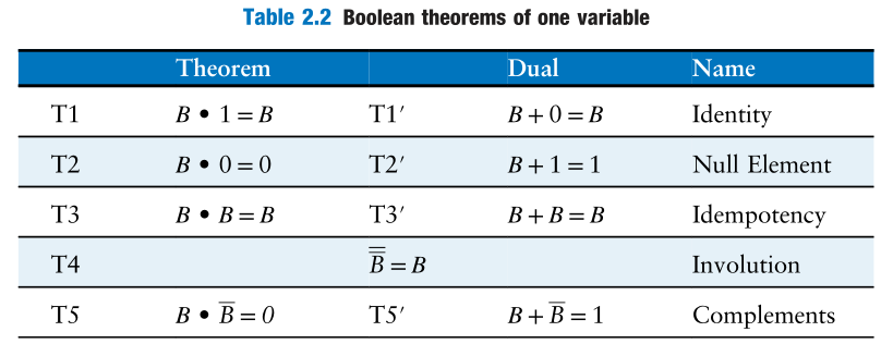
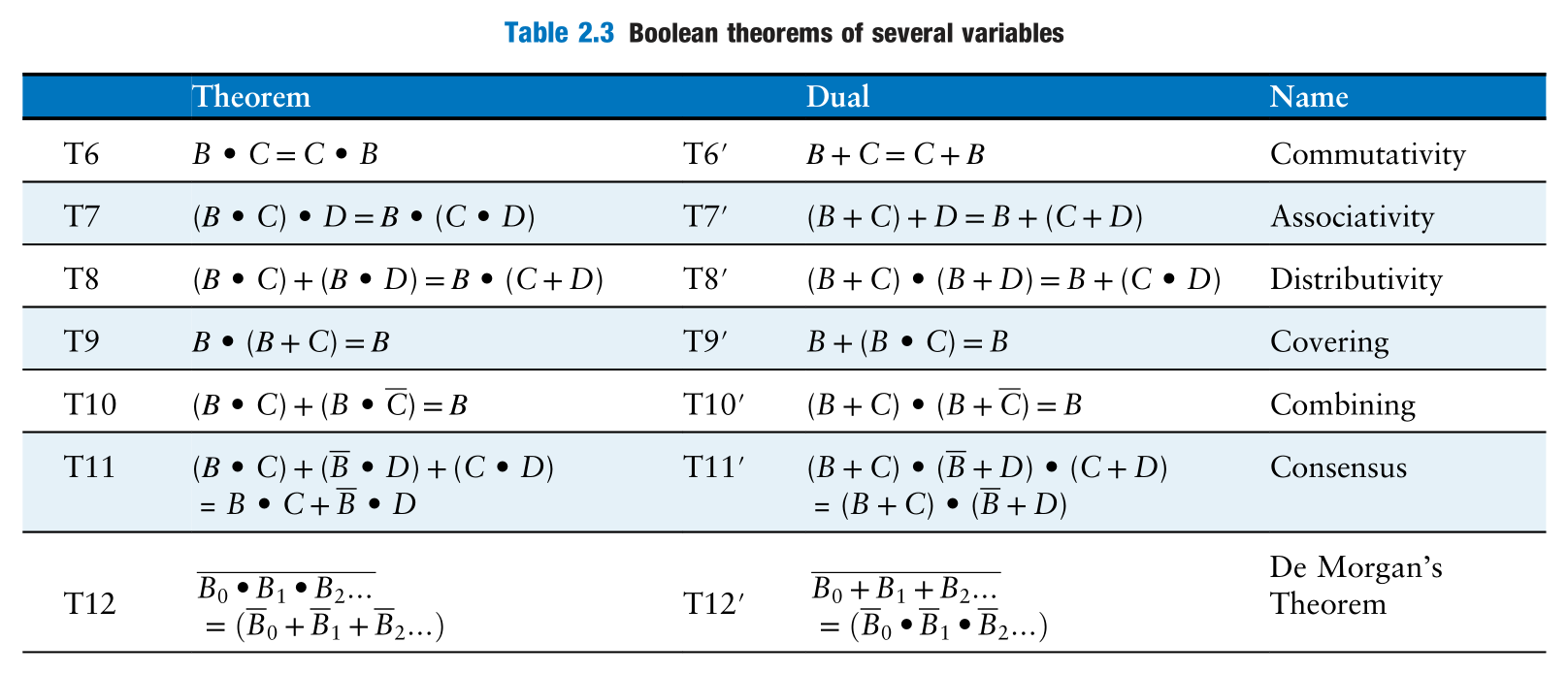
Theorems
3 构建组合逻辑电路
Rules for bubble pushing
According to the theorems, the underlying rules for bubble pushing are
- Pushing bubbles backward (from the output) or forward (from the inputs) changes the body of the gate from AND to OR or vice versa.
- Pushing a bubble from the output back to the inputs puts bubbles on all gate inputs.
- Pushing bubbles on all gate inputs forward toward the output puts a bubble on the output.
Drawing Schematics
A schematic is a diagram of a digital circuit showing the elements and the wires that connect them together.
By drawing schematics in a consistent fashion, we make them easier to read and debug. We will generally obey the following guidelines:
- Inputs are on the left (or top) side of a schematic.
- Outputs are on the right (or bottom) side of a schematic.
- Whenever possible, gates should flow from left to right.
- Straight wires are better to use than wires with multiple corners (jagged wires waste mental effort following the wire rather than thinking of what the circuit does).
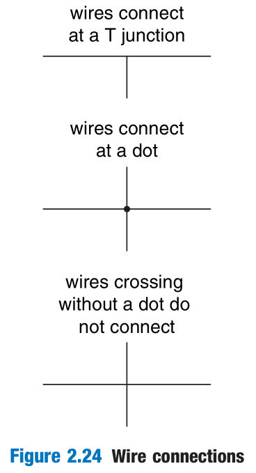
- Wires always connect at a T junction.
- A dot where wires cross indicates a connection between the wires.
- Wires crossing without a dot make no connection.
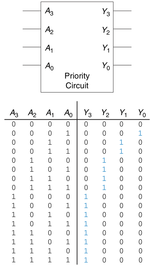
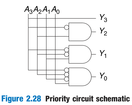
Priority Circuit
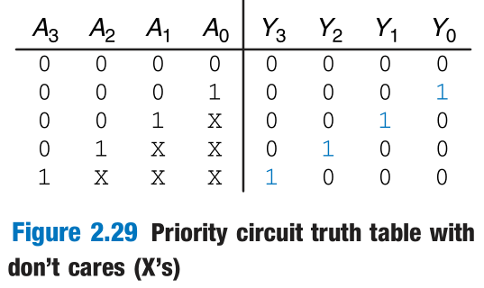
We use the symbol X to describe inputs that the output doesn’t care about.
Bubble Pushing
The guidelines for bubble pushing are as follows:
Begin at the output of the circuit and work toward the inputs.
Push any bubbles on the final output back toward the inputs so that you can read an equation in terms of the output (for example, $Y$) instead of the complement of the output $\overline Y$.
Working backward, draw each gate in a form so that bubbles cancel.
If the current gate has an input bubble, draw the preceding gate with an output bubble. If the current gate does not have an input bubble, draw the preceding gate without an output bubble.
Illegal Value and Floating Value
The symbol X indicates that the circuit node has an unknown or illegal value. This commonly happens if it is being driven to both 0 and 1 at the same time.
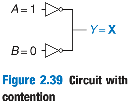
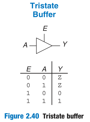
The symbol Z indicates that a node is being driven neither HIGH nor LOW. The node is said to be floating, high impedance, or high Z.
A floating node might be 0, might be 1, or might be at some voltage in between, depending on the history of the system.
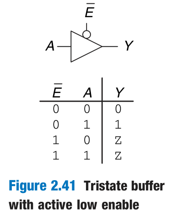
The tristate buffer, shown in Figure 2.40, has three possible output states: HIGH (1), LOW (0), and floating (Z).
4 卡诺图
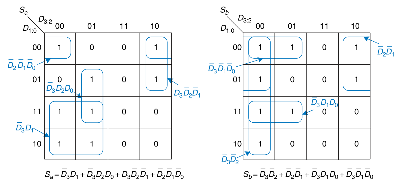
Karnaugh maps (K-maps) are a graphical method for simplifying Boolean equations.

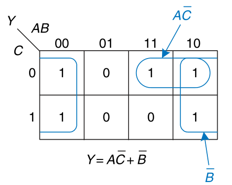
Adjacent squares share all the same literals except one, which appears in true form in one square and in complementary form in the other. You may have noticed that the A and B combinations in the top row are in a peculiar order: 00, 01, 11, 10. This order is called a Gray code.
The K-map also “wraps around.”
Logic Minimization with K-Maps
K-maps provide an easy visual way to minimize logic. Rules for finding a minimized equation from a K-map are as follows:
- Use the fewest circles necessary to cover all the 1’s.
- All the squares in each circle must contain 1’s.
- Each circle must span a rectangular block that is a power of 2 (i.e., 1, 2, or 4) squares in each direction.
- Each circle should be as large as possible.
- A circle may wrap around the edges of the K-map.
- A 1 in a K-map may be circled multiple times if doing so allows fewer circles to be used.
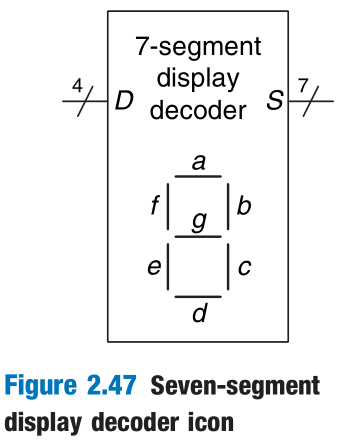
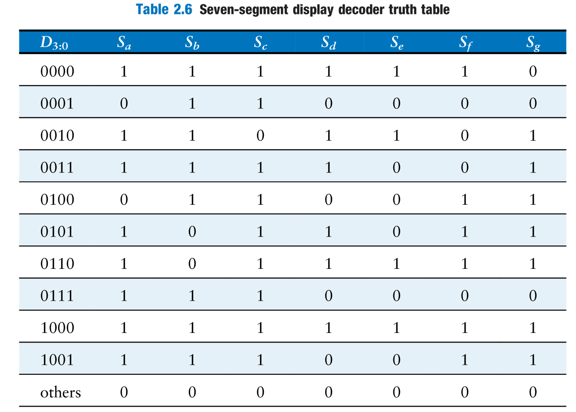
Seven-segment Display Decoder
Don‘t Cares
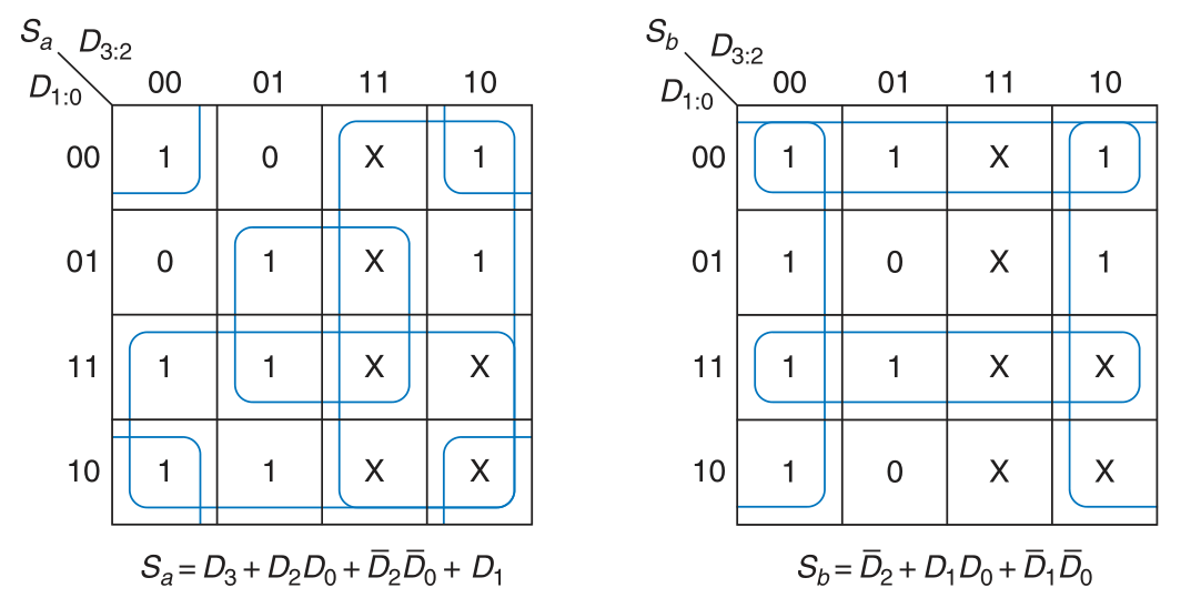
Don’t cares also appear in truth table outputs where the output value is unimportant or the corresponding input combination can never happen. Such outputs can be treated as either 0’s or 1’s at the designer’s discretion.
5 组合逻辑模块
Multiplexers
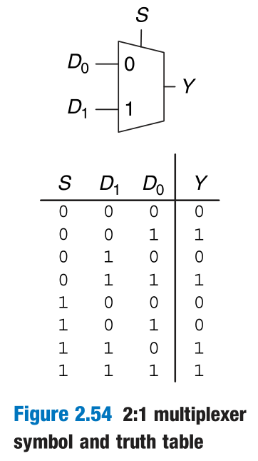
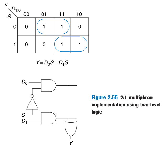
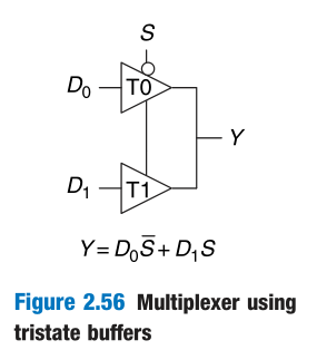
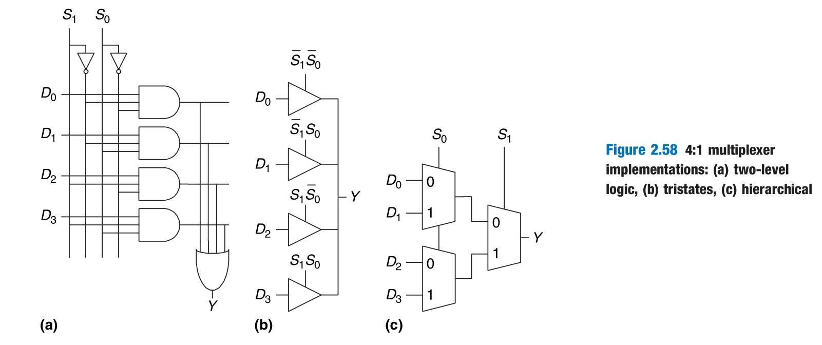
Multiplexer Logic
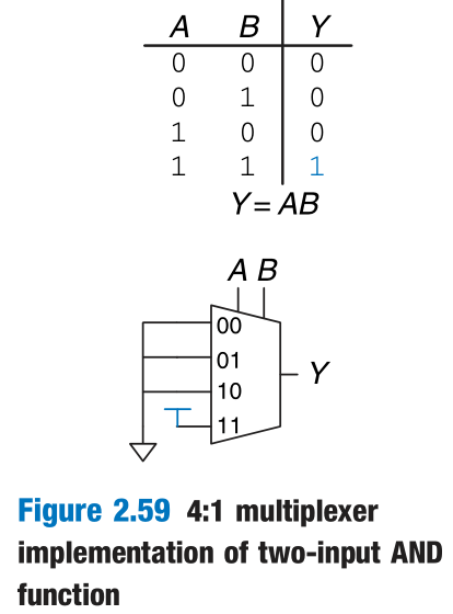
Multiplexers can be used as lookup tables to perform logic functions.
In general, a $2^N$-input multiplexer can be programmed to perform any N-input logic function by applying 0’s and 1’s to the appropriate data inputs.
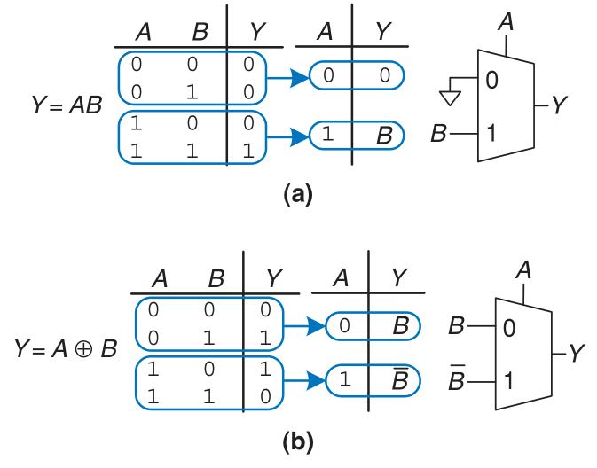
With a little cleverness, we can cut the multiplexer size in half, using only a $2^{N-1}$-input multiplexer to perform any N-input logic function.
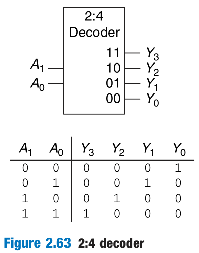
Decoder
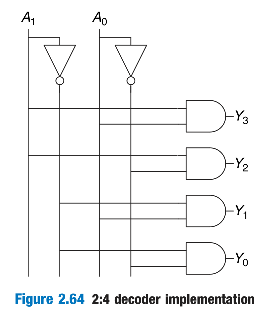
Decoder Logic
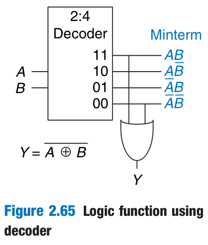
When using decoders to build logic, it is easiest to express functions as a truth table or in canonical sum-of-products form. An N-input function with M 1’s in the truth table can be built with an N:2N decoder and an M-input OR gate attached to all of the minterms containing 1’s in the truth table.
5 Timing
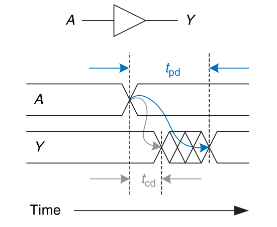
Propagation and Contamination Delay
The propagation delay $t_{pd}$ is the maximum time from when an input changes until the output or outputs reach their final value.
The contamination delay $t_{cd}$ is the minimum time from when an input changes until any output starts to change its value.
Critical Path and Short Path
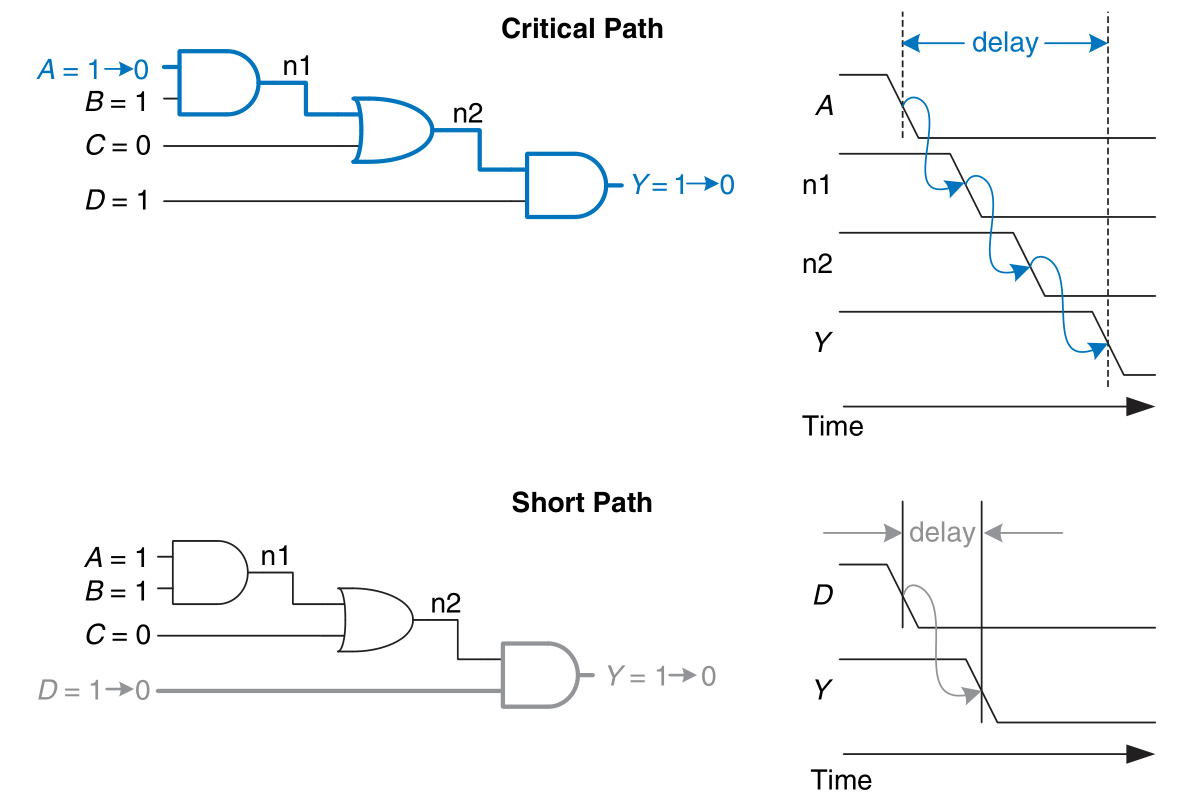
The critical path limits the speed at which the circuit operates.
The short path is the fastest path through the circuit.
The propagation delay of a combinational circuit is the sum of the propagation delays through each element on the critical path.
The contamination delay is the sum of the contamination delays through each element on the short path.
Glitches
It is possible that a single input transition can cause multiple output transitions. These are called glitches or hazards.
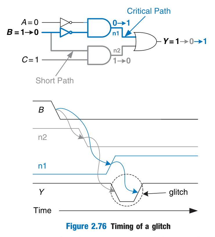
In general, a glitch can occur when a change in a single variable crosses the boundary between two prime implicants in a K-map. We can eliminate the glitch by adding redundant implicants to the K-map to cover these boundaries. This of course comes at the cost of extra hardware.
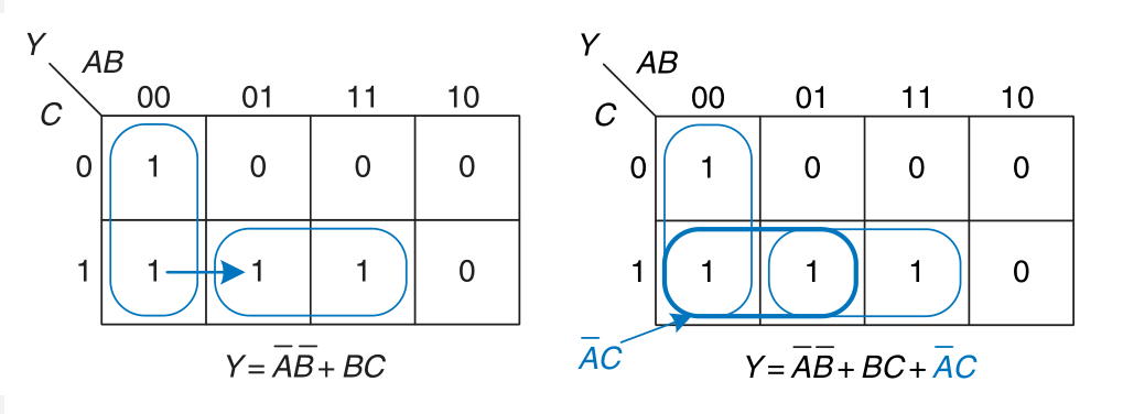
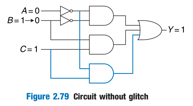
However, simultaneous transitions on multiple inputs can also cause glitches. These glitches cannot be fixed by adding hardware.
Digital Design and Computer Architecture 第二章归纳
http://example.com/2022/07/22/Digital-Design-and-Computer-Architecture-第二章归纳/